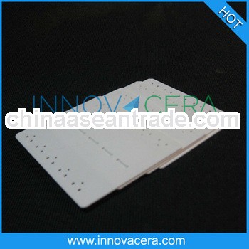
96 Al2O3/High Frequency Ceramics/Substrate/Innovacera
Innovacera have been developed by combining metallization and ceramic material technologies which MARUWA has cultivated for many years. The materials can be customized with various pattern technologies, such as wraparound metallization. This product is used in circuit substrates for optical storage, optical communication, RF application, and various other uses.
The base layer is tungsten or moly-manganese, screen printed with a minimum layer thickness of 6 µm. An electrolytic nickel layer (approximately 2 µm) assures a good solder flow. Other thicknesses are available for specific customer requirements. Electrolytic nickel plating requires electrical connections for the plating process. Special design guidelines will therefore apply wherever an electrolytic technique is involved.
An optional gold flash layer (approximately 0,1 µm) may be added to enhance corrosion resistance. As a further option, the electrolytic nickel layer may be covered with bondable gold plating. Solder finishes are also available.
Overview of Main Physical Properties:
1.Good electrical insulation
2.High mechanical strength
3.Excellent wear resistance
4.Excellent corrosion resistance
5.Low dielectric constant
Overview of Main Applications:
1. High Power LED ceramic substrate
2. Microwave (Wireless Communication & Radar)
3. Semiconductor Process Equipment
4. Solar Cell
5. Hybrid Electric Vehicles
6. Flip chip/eutectic substrate
7. Sensor ceramic substrate
5. Properties of Alumina Al2O3
Now our Office
We are specialized in the Ceramic tubes manufacturing.If you need any help about is,please don't hesitate to contact with us.


